Introduction
Definition: A Buck Converter is a type of DC-DC converter that steps down a higher input DC voltage to a lower output DC voltage. That is, the output voltage is always less than the input voltage.
\[ V_{out} = D \, V_{in} \]Where, D is the duty cycle.
It is also called a Step-Down DC-DC Converter, Step-Down Chopper, or Buck Regulator. The name “Buck” originates from the fact that the inductor in the circuit “Bucks” or opposes the input voltage.
The buck converter efficiently converts a higher DC input voltage \( V_{\mathrm{in}} \) into a lower, regulated DC output voltage \( V_{\mathrm{out}} \). This is achieved through high-frequency switching, where an electronic switch alternately connects and disconnects the input source to an energy-storage element, typically an inductor.
The switch is controlled using Pulse-Width Modulation (PWM), which regulates the average output voltage by adjusting the ON and OFF durations of the switch.
Why Do We Need DC–DC Conversion?
Many electronic systems require DC voltages different from what is directly available from the source. Common scenarios include:
- Battery systems (Fixed voltage) supplying electronics that need regulated, lower voltages.
- Electric drives that require variable DC voltages for motor speed control.
- Power supplies for embedded systems, telecom, and automotive electronics.
DC-DC converters, or choppers, efficiently provide this flexibility by switching power devices between nearly-zero and low-impedance states, minimizing conduction and switching losses when designed properly.
Operating Principle of Buck Converter
The operation of the buck converter is based on the principle of storing energy in an inductor. The voltage drop across an inductor is proportional to the change in the electric current flowing through the device. A switching transistor is used between input and output and switches continuously ON and OFF at high frequency. To maintain a continuous output, the circuit uses the energy stored in the inductor.
The solid-state device (Like BJT, MOSFET, IGBT, etc.) acts as a switch for the circuit. There is another switch in the circuit which is a Freewheeling or Flywheel Diode (FD). The combination of these two switches forms a connection with a low-pass LC filter in order to reduce current or voltage ripples. This helps in generating a regulated DC output. A pure resistor is connected across this whole arrangement that acts as the load of the circuit. {fig:ckt_buck_converter} given below shows the circuit representation of the Buck Converter.
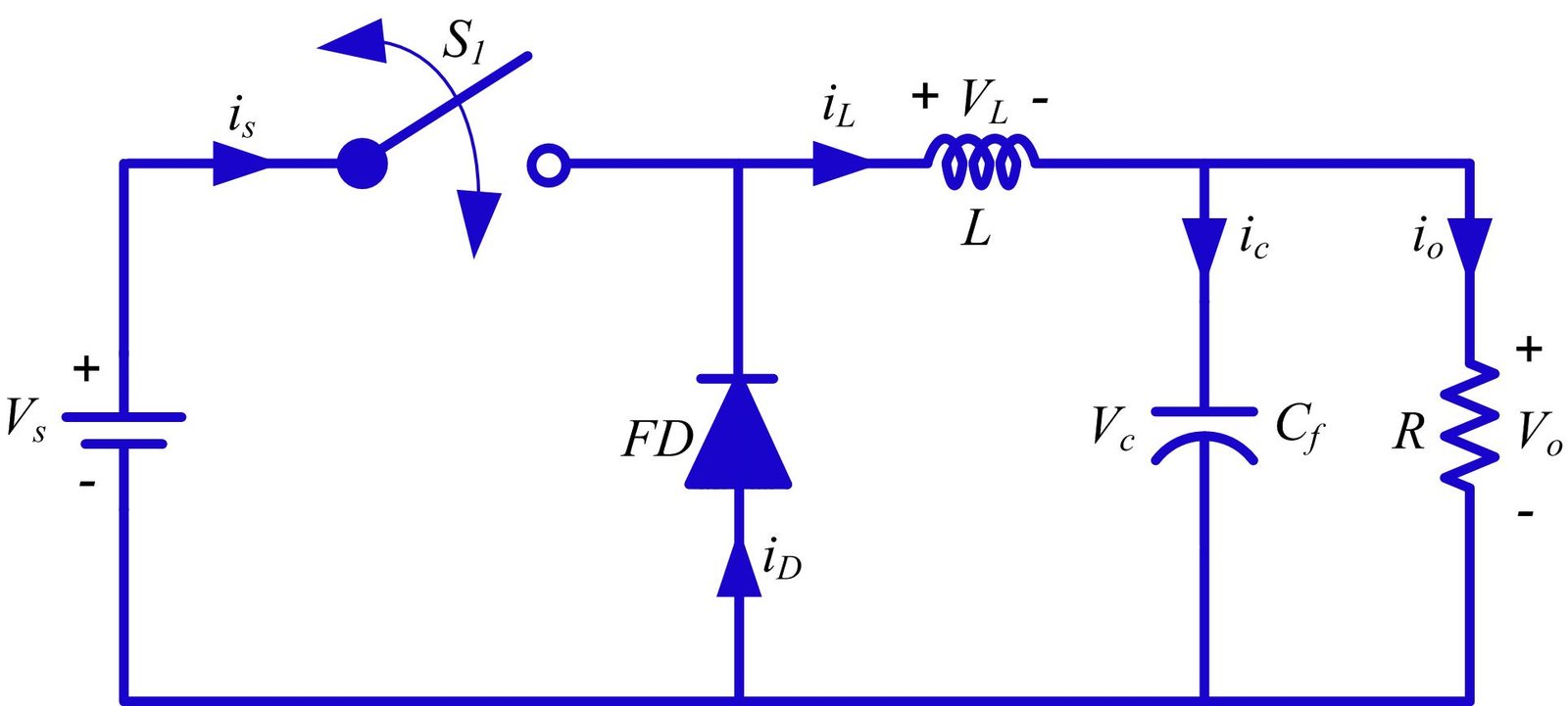
The controlled switch is turned on and off by using PWM (Pulse Width Modulation). PWM can be time-based or frequency-based. Time-based modulation is mostly used for buck converters because it is simple to construct and use. The switching frequency remains constant in time-based PWM. Whereas frequency-based modulation introduces variable frequency and often complicates LC filter design.
However, due to Lenz's law, the energy stored within the inductor will oppose the cause which produced it, so an induced current will be generated and the polarity across the inductor will be reversed when the switch changes state.
The Buck Converter circuit consists of the switching transistor together with the Freewheeling or Flywheel Diode (FD) circuit. The whole operation of the circuit can be divided into two modes:
- Mode I: Switch \(S_1\) is ON and Diode \(F_D\) is OFF.
- Mode II: Switch \(S_1\) is OFF and Diode \(F_D\) is ON.
Mode 1: Switch \(S_1\) is ON and Diode \(F_D\) is OFF \((0 \le t \le T_{\mathrm{ON}})\)
In this mode of operation, the power MOSFET (i.e., switch \(S_1\)) is closed and therefore the freewheeling diode (FD) is reverse biased by the supply voltage \(V_s\) and therefore FD acts as an open switch. Thus switch \(S_1\) allows the flow of current through it. The circuit diagram for this mode is shown in {fig:ckt1_buck_converter}
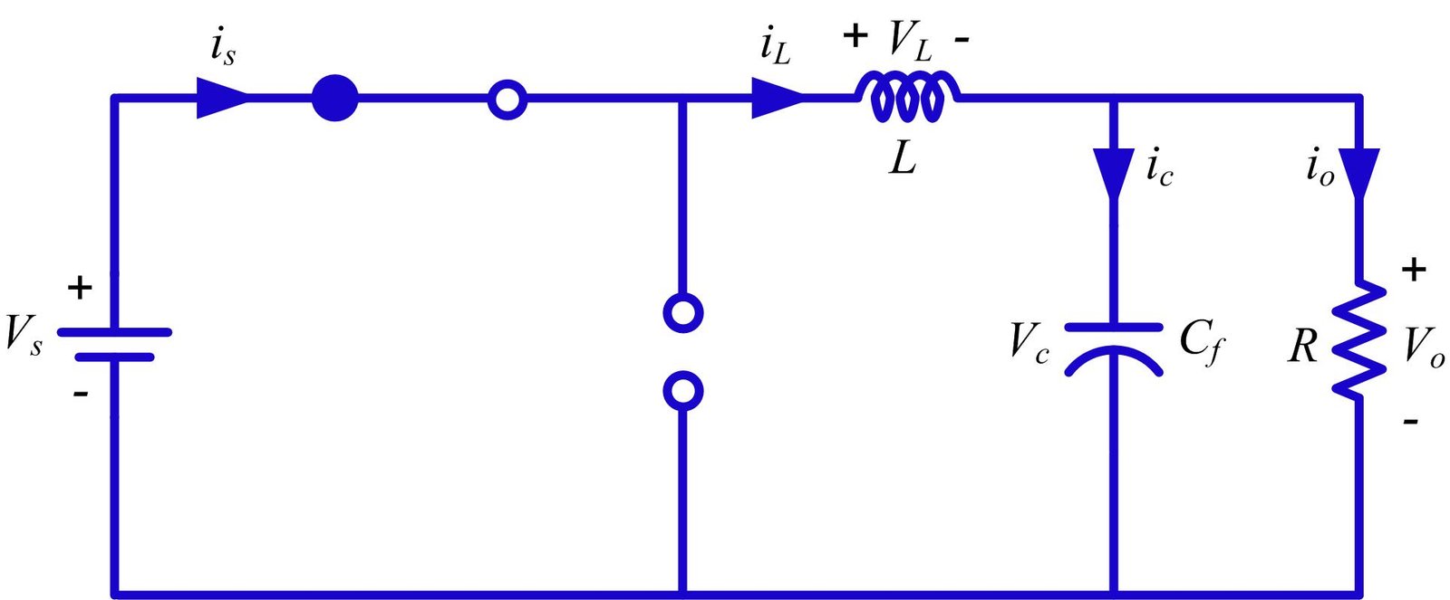
When a constant dc voltage is applied across the input terminal of the circuit, current flows while the switch \(S_1\) is closed whereas the diode FD is reverse biased. Due to this current flow, the inductor \(L\) stores energy in the form of a magnetic field. The capacitor also stores charge. The input voltage \(V_s\) is applied to the switching node, and the inductor sees the difference between the input and output voltages, as shown in {fig:ckt1_buck_converter}
Thus, during this interval the inductor voltage is:
\[ V_L = V_s - V_o \]Let us assume that during one complete switching cycle, the switch \(S_1\) remains in the ON state for a duration of \(T_{ON}\) and in the OFF state for a duration of \(T_{OFF}\). The total switching period is
\[ T = T_{ON} + T_{OFF} \]The duty cycle \(D\) is defined as:
\[ D = \frac{T_{ON}}{T} \]Where,
- \( T_{ON} \) is the ON interval
- \( T_{OFF} \) is the OFF interval
- \( V_s \) is the source or input voltage
- \( V_o \) is the output or load voltage
- \( T \) is the chopping period
Inductor Current Ripple \(\Delta i_L\) of an Ideal Buck Converter (CCM) During \(D T_s\)
The voltage across an inductor is related to the rate of change of current through it. By definition we know:
\begin{equation} V_L = L \frac{di_L}{dt} \label{eq:inductor_voltage_law} \end{equation}ON Interval, Switch Closed, Duration \(D T_s\)
Applying Kirchhoff’s Voltage Law (KVL) around the loop when the switch \(S_1\) is closed:
\begin{equation} V_L = V_s - V_o \label{eq:on_inductor_voltage} \end{equation}Substituting equation \(\eqref{eq:on_inductor_voltage}\) into equation \(\eqref{eq:inductor_voltage_law}\), write the ordinary differential equation (ODE) and separate variables:
\[ L \frac{di_L}{dt} = V_s - V_o \] \[ \frac{di_L}{dt} = \frac{V_s - V_o}{L} \] \[ di_L = \frac{V_s - V_o}{L}\, dt \]Now integrate both sides over the ON interval. Choose the time limits \(t=0\) (Start of period) to \(t = D T_s\) (End of ON interval). Corresponding current limits are \(i_L(0)\) to \(i_L(DT_s)\).
\[ \int_{i_L(0)}^{\,i_L(DT_s)} \,di_L \;=\; \int_{0}^{\,D T_s} \frac{V_s - V_o}{L}\,dt \]Evaluate both integrals explicitly:
Left side:
\[ \int_{i_L(0)}^{i_L(DT_s)} \,di_L = i_L(DT_s) - i_L(0) \]Right side: Integrand is constant in time, so
\[ \int_{0}^{D T_s} \frac{V_s - V_o}{L}\, dt = \frac{V_s - V_o}{L} \int_{0}^{D T_s} dt = \frac{V_s - V_o}{L}\, D T_s \]Equate the two results to obtain the current change during the ON interval:
\begin{equation} i_L(DT_s) - i_L(0) = \frac{V_s - V_o}{L}\,D T_s \label{eq:on_current_change} \end{equation}Define the change in inductor current:
\begin{equation} \Delta i_L = i_L(DT_s) - i_L(0) \label{eq:on_ripple_definition} \end{equation}Substituting equation \(\eqref{eq:on_ripple_definition}\) into equation \(\eqref{eq:on_current_change}\), we obtain:
\begin{equation} \boxed{\Delta i_L = \frac{V_s - V_o}{L} \, D T_s} \label{eq:delta_on} \end{equation}Mode 2: Switch \(S_1\) is OFF and Diode \(F_D\) is ON \((T_{\mathrm{ON}} \le t \le T)\)
The second mode of operation begins when the switch \(S_1\) is turned OFF. As a result, the inductor-which had stored energy during the previous interval-now releases this stored energy by acting as a source. The polarity of the inductor voltage reverses, which forward-biases the freewheeling diode \(FD\) and allows it to conduct automatically.
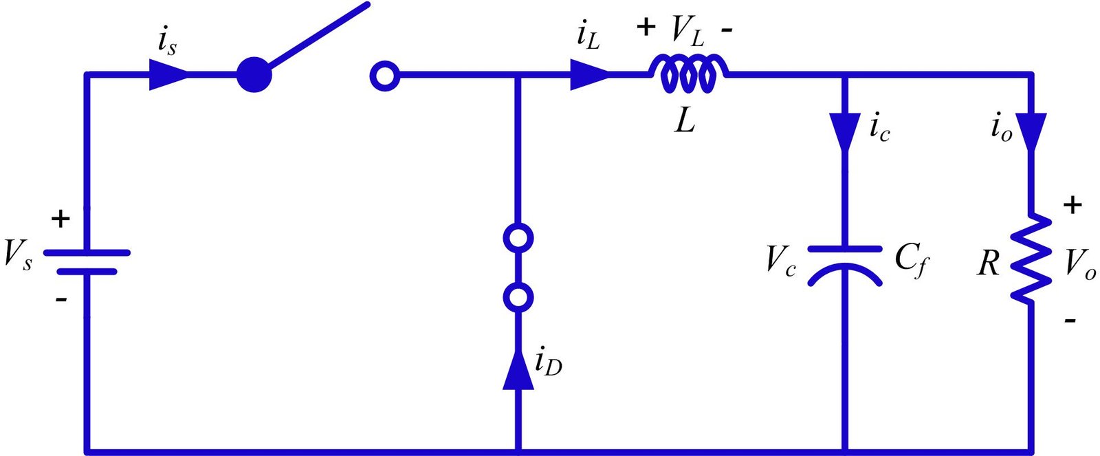
During this period, the switch \(S_1\) remains open (Non-conducting), while the diode \(FD\) provides a closed path for the inductor current. The corresponding circuit diagram for this mode of operation is shown in {fig:ckt2_buck_converter}
When the switch is OFF, the switching-node voltage is zero for an ideal freewheeling path, while the output capacitor maintains the load voltage. Therefore, the inductor voltage is:
\begin{equation} V_L = -V_o \label{eq:off_inductor_voltage} \end{equation}The inductor releases the energy stored in its magnetic field during the ON period. Since the polarity of the inductor reverses, it maintains the flow of current through the load via the conducting diode \(FD\). This conduction continues until the inductor has completely discharged its stored energy.
In continuous conduction mode (CCM), the inductor current decreases during this interval but remains greater than zero. At the start of the next switching cycle, switch \(S_1\) turns ON again and the diode becomes reverse-biased.
Inductor Current Ripple \(\Delta i_L\) of an Ideal Buck Converter (CCM) During \((1-D)T_s\)
The voltage-current relationship of the inductor is given by equation \(\eqref{eq:inductor_voltage_law}\).
OFF Interval, Switch Open, Duration \((1-D)T_s\)
Applying Kirchhoff’s Voltage Law (KVL), when the switch is OFF, the inductor voltage, assuming an ideal diode or synchronous rectifier, is:
\begin{equation} V_L + V_o = 0 \label{eq:off_kvl_loop} \end{equation}Rearranging equation \(\eqref{eq:off_kvl_loop}\) gives the OFF-state inductor voltage already stated in equation \(\eqref{eq:off_inductor_voltage}\).
Using equations \(\eqref{eq:inductor_voltage_law}\) and \(\eqref{eq:off_inductor_voltage}\), write the ODE and separate variables:
\[ L \frac{di_L}{dt} = -V_o \] \[ \frac{di_L}{dt} = -\frac{V_o}{L} \] \[ di_L = -\frac{V_o}{L}\,dt \]Integrate both sides over the OFF interval. Use time limits \(t = D T_s\) to \(t = T_s\). Current limits are \(i_L(DT_s)\) to \(i_L(T_s)\):
\[ \int_{i_L(DT_s)}^{\,i_L(T_s)} \,di_L \;=\; \int_{D T_s}^{\,T_s} -\frac{V_o}{L}\,dt \]Evaluate both integrals explicitly:
Left side:
\[ \int_{i_L(DT_s)}^{i_L(T_s)} \,di_L = i_L(T_s) - i_L(DT_s) \]Right side:
\[ \int_{D T_s}^{T_s} -\frac{V_o}{L}\,dt = -\frac{V_o}{L} \int_{D T_s}^{T_s} dt = -\frac{V_o}{L} (T_s - D T_s) = -\frac{V_o}{L} (1-D) T_s \]Equate the two results to obtain the current change during the OFF interval:
\begin{equation} i_L(T_s) - i_L(DT_s) = -\frac{V_o}{L}(1-D)T_s \label{eq:off_current_change} \end{equation}Define the change in inductor current:
\begin{equation} \Delta i_L = i_L(T_s) - i_L(DT_s) \label{eq:off_ripple_definition} \end{equation}Substituting equation \(\eqref{eq:off_ripple_definition}\) into equation \(\eqref{eq:off_current_change}\), the current change during the OFF interval is:
\begin{equation} \boxed{\Delta i_L = -\frac{V_o}{L}(1-D)T_s} \label{eq:delta_off} \end{equation}Steady-State Periodic Condition
In the steady-state operation of a buck converter, the inductor current at the end of one switching period is equal to the inductor current at the beginning of that period:
\[ i_L(T_s) = i_L(0) \]This means that over a complete switching cycle, the net change in the inductor current is zero. Summing the voltage-time (volt-second) contributions during the ON and OFF intervals and setting their sum equal to zero gives:
\begin{equation} \Delta i_{L,\mathrm{ON}} + \Delta i_{L,\mathrm{OFF}} = 0 \label{eq:ripple_balance} \end{equation}Substituting equations \(\eqref{eq:delta_on}\) and \(\eqref{eq:delta_off}\) (the ON and OFF ripple expressions) into equation \(\eqref{eq:ripple_balance}\), we get:
\begin{equation} \frac{V_s - V_o}{L} D T_s \;-\; \frac{V_o}{L} (1 - D) T_s = 0 \label{eq:volt_second_substitution} \end{equation}Simplifying equation \(\eqref{eq:volt_second_substitution}\) yields the standard volt-second balance relation:
\begin{equation} \boxed{ V_o = D \, V_s } \label{eq:voltage_gain} \end{equation}Derivation of Inductor and Capacitor in Buck Converter
In Continuous Conduction Mode (CCM), the inductor current waveform is triangular in shape, consisting of a ripple component \(\Delta i_L\) superimposed on the average current \(i_L\). The inductor current increases during the ON interval (\(T_{\mathrm{ON}}\)) and decreases during the OFF interval (\(T_{\mathrm{OFF}}\)).
Inductor Current Ripple \(\Delta i_L\) and Inductor Selection
From the ON-state ripple in equation \(\eqref{eq:delta_on}\), the peak-to-peak inductor-current ripple can be expressed in design form as:
\begin{equation} \Delta i_L = \frac{(V_s - V_o) D T}{L} \label{eq:inductor_ripple_design} \end{equation}Rearranging equation \(\eqref{eq:inductor_ripple_design}\) for the inductance \(L\) gives:
\[ L \, \Delta i_L = (V_s - V_o) D T \] \begin{equation} \boxed{ L = \frac{(V_s - V_o) D T}{\Delta i_L} } \label{eq:inductance_period} \end{equation}Substituting \(T = \dfrac{1}{f_s}\) into equation \(\eqref{eq:inductance_period}\), the inductance can also be expressed as:
\begin{equation} \boxed{ L = \frac{(V_s - V_o) D}{\Delta i_L f_s} } \label{eq:inductance_frequency} \end{equation}During the OFF interval, the inductor current decreases, and the corresponding current ripple magnitude can be written as:
\begin{equation} \Delta i_L = \frac{V_o}{L} (1 - D) T \label{eq:off_ripple_magnitude} \end{equation}Rearranging equation \(\eqref{eq:off_ripple_magnitude}\) for \(L\) yields another useful expression:
\begin{equation} \boxed{ L = \frac{V_o (1 - D)}{\Delta i_L f_s} } \label{eq:inductance_off} \end{equation}Capacitor Voltage Ripple \(\Delta v_c\) and Capacitor Selection
The relationship between the capacitor current and its voltage is given by:
\begin{equation} i_c(t) = C \frac{d v_c}{dt} \label{eq:capacitor_current} \end{equation}Rearranging equation \(\eqref{eq:capacitor_current}\), we can write:
\begin{equation} \frac{dv_c}{dt} = \frac{i_c(t)}{C} \quad\Rightarrow\quad dv_c = \frac{i_c(t)}{C} \, dt \label{eq:capacitor_voltage_rate} \end{equation}Let the inductor current have a peak-to-peak ripple denoted by \(\Delta i_L\). The inductor current waveform is triangular, with its peak value above the average current by \(\dfrac{\Delta i_L}{2}\) and its minimum value below the average by \(-\dfrac{\Delta i_L}{2}\). The two time instants when \(i_L(t)\) equals the average current \(I_L\) are:
\[ t_1 = \frac{D T_s}{2}, \qquad t_2 = \frac{(1 + D) T_s}{2} \]The duration for which \(i_c(t) > 0\) (i.e., when \(i_L > I_L\)) is given by \(t_2 - t_1 = \dfrac{T_s}{2}\). During this interval, the capacitor current waveform is a triangle with a base of \(\dfrac{T_s}{2}\) and a height of \(\dfrac{\Delta i_L}{2}\).
The area of this positive triangular portion (representing the charge transferred to the capacitor) is given by:
\begin{equation} \text{Area}_+ = \frac{1}{2} \cdot \frac{T_s}{2} \cdot \frac{\Delta i_L}{2} = \frac{\Delta i_L \, T_s}{8} \label{eq:positive_charge_area} \end{equation}By the principle of charge balance, the charge in equation \(\eqref{eq:positive_charge_area}\) equals the change in capacitor voltage over one ripple cycle, that is:
\begin{equation} C \, \Delta v_c = \frac{\Delta i_L \, T_s}{8} \label{eq:capacitor_charge_balance} \end{equation}Rearranging equation \(\eqref{eq:capacitor_charge_balance}\), the capacitor voltage ripple is obtained as:
\begin{equation} \boxed{ \Delta v_c = \frac{\Delta i_L \, T_s}{8 C} } \label{eq:capacitor_ripple} \end{equation}Applications
A Buck converter is primarily used for converting a high DC voltage into a lower DC voltage. Its major applications include:
- Battery-powered systems such as battery chargers for mobile phones, laptops, and power banks.
- Self-regulating power supplies such as Switch Mode Power Supplies (SMPS).
- Point-of-load converters for PCs and motherboards.
- Solar charging systems.
- Adaptive control applications.
- Power audio amplifier circuits.
Conclusion
The Buck Converter, also known as a step-down DC–DC converter, efficiently converts a higher DC input voltage into a lower regulated output voltage using high-frequency switching and energy storage in inductors and capacitors. By analyzing its operating modes, the converter’s steady-state relationship in equation \(\eqref{eq:voltage_gain}\) was derived, demonstrating that the output voltage is directly proportional to the duty cycle of the switching signal.
Further, the integration of inductor current ripple and capacitor voltage ripple provided insights into the selection of \( L \) and \( C \) values for minimizing current and voltage ripples, ensuring stable operation in continuous conduction mode (CCM).
In summary, the buck converter represents one of the most fundamental and efficient DC–DC converter topologies, widely used in applications such as power supplies, battery systems, solar chargers, and embedded electronics, where regulated step-down voltage is essential.
Important Questions
- What is a buck converter, and why is it called a step-down DC–DC converter?
Answer: A buck converter is a switched-mode power converter that changes a higher DC input voltage into a lower regulated DC output voltage. It is called a step-down converter because, ideally, \(V_o = D V_s\), where \(0 < D < 1\); therefore, \(V_o < V_s\).
- Draw the circuit diagram of an ideal buck converter and explain the function of each component.
Answer: The circuit consists of a controlled switch, freewheeling diode, inductor, capacitor, and load. The switch controls input-energy transfer, the diode provides an inductor-current path while the switch is OFF, the inductor limits current ripple and stores energy, and the capacitor smooths the output voltage.
- Explain the operation of a buck converter during the switch ON interval.
Answer: The switch conducts and the diode is reverse-biased. The source supplies the load and stores energy in the inductor. The inductor voltage is \(V_L = V_s - V_o\), so its current increases linearly.
- Explain the operation of a buck converter during the switch OFF interval.
Answer: The switch opens and the diode conducts. The inductor releases its stored energy through the diode, capacitor, and load. The inductor voltage is \(V_L = -V_o\), so its current decreases linearly while remaining continuous in CCM.
- Draw and explain the gate-pulse, inductor-voltage, inductor-current, diode-current, and output-voltage waveforms.
Answer: The gate pulse is high for \(DT_s\) and low for \((1-D)T_s\). Inductor voltage alternates between \(V_s-V_o\) and \(-V_o\). Inductor current is triangular, switch current flows during the ON interval, diode current flows during the OFF interval, and output voltage is nearly constant with a small ripple.
- What is Continuous Conduction Mode (CCM), and what condition must the inductor current satisfy in CCM?
Answer: CCM is the operating mode in which inductor current flows throughout the complete switching cycle. Its minimum value must remain greater than zero: \(I_{L,\min}>0\).
- Explain how switching frequency, inductance, and capacitance affect the current and voltage ripples.
Answer: Inductor-current ripple is inversely proportional to \(L\) and \(f_s\), while capacitor-voltage ripple is inversely proportional to \(C\) and \(f_s\). Therefore, increasing switching frequency, inductance, or capacitance reduces ripple, although it can increase cost, size, or switching loss.
- The buck-converter output voltage is lower than expected. What would you check first?
Answer: Check the input voltage, PWM duty cycle, load current, current-limit status, feedback-divider values, and output for a short circuit. Then inspect MOSFET gate drive, diode polarity, inductor saturation, and voltage drops using an oscilloscope and multimeter.
- Why might a buck converter become very hot even though the output voltage is correct?
Answer: Possible causes include excessive load current, high MOSFET conduction or switching loss, an undersized or saturating inductor, a slow diode, poor PCB layout, insufficient gate drive, high capacitor ESR, or inadequate copper area and airflow.
- How would you choose an inductor for a practical buck converter?
Answer: Select inductance for an acceptable ripple current, then verify that saturation current exceeds the peak inductor current and RMS-current rating exceeds the operating current. Also consider DCR, core loss, size, temperature rise, tolerance, and switching frequency.
- How would you choose the output capacitor?
Answer: Choose capacitance and ESR to meet voltage-ripple and transient-response requirements. Verify voltage rating, ripple-current rating, temperature behavior, lifetime, tolerance, and compatibility with the controller's loop-stability requirements.
- What is the difference between a synchronous and a non-synchronous buck converter?
Answer: A non-synchronous buck uses a diode as the low-side device, while a synchronous buck replaces it with a controlled MOSFET. Synchronous designs generally improve efficiency at low output voltages and high currents but require more complex gate timing to prevent shoot-through.
- Why is PCB layout critical in a buck converter?
Answer: High \(di/dt\) current loops and high \(dv/dt\) switching nodes can create ringing, EMI, noise, and excess device stress. Keep the input capacitor, switches, diode, and ground-return loop compact; minimize the switch-node copper area; and route feedback away from noisy power paths.
- How would you measure output ripple correctly with an oscilloscope?
Answer: Use AC coupling when appropriate, enable a suitable bandwidth limit, and connect the probe with a short ground spring directly across the output capacitor. A long probe ground lead forms an antenna and can show misleading switching spikes.
- What happens when the inductor saturates?
Answer: Its effective inductance drops sharply, causing current to rise rapidly. This can increase ripple and temperature, trigger current limiting, collapse the output, or damage the MOSFET, diode, or inductor.
- What protections should a production buck converter include?
Answer: Common protections include input undervoltage lockout, cycle-by-cycle overcurrent limiting, short-circuit protection, output overvoltage protection, thermal shutdown, soft start, reverse-polarity protection, and controlled recovery from faults.
- Why is soft start used?
Answer: Soft start gradually increases the reference or duty cycle during startup. It limits inrush current, reduces output overshoot, prevents input-voltage collapse, and lowers stress on the switch, inductor, diode, and capacitor.
- How can you improve buck-converter efficiency?
Answer: Use low-loss MOSFETs, an appropriate switching frequency, a low-DCR inductor, low-ESR capacitors, an efficient gate driver, synchronous rectification where beneficial, short current loops, and adequate thermal design. Optimize components for the actual input, output, and load range.
- List the advantages and practical applications of a buck converter.
Answer: Advantages include high efficiency, compact size, adjustable output, and low heat loss. Applications include battery chargers, point-of-load regulators, computers, embedded systems, solar chargers, DC motor drives, and switch-mode power supplies.
References
- Robert W. Erickson and Dragan Maksimović, Fundamentals of Power Electronics.
- Ned Mohan, Tore M. Undeland, and William P. Robbins, Power Electronics: Converters, Applications, and Design.
- Muhammad H. Rashid, Power Electronics: Circuits, Devices, and Applications.
- Electrical4U
- TutorialsPoint
- Circuit Globe
- All About Circuits
- GeeksforGeeks
- Analog Devices

Hi! I'm Antu, Creator of This Project. I Completed My M.Tech in Power Electronics from NIT_Calicut. I Pursue My Passion for Innovation and Technology. I Love Exploring Electrical and Electronic Systems, Learning and Sharing Knowledge.
"Embrace Risks In Your Work. Even If You Don't Achieve The Desired Output, You'll Always Gain Valuable Lessons."